
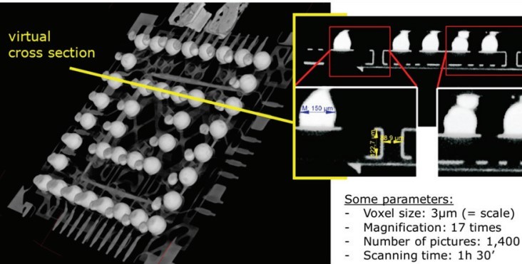
Advanced electronics packaging is a challenge for non-destructive Testing (NDT). More, smaller and mostly hidden interconnects dominate modern electronics components and systems. To solve the demands of customers to get products with a high functionality by low volume, weight and price (e.g. mobile phones, personal medical monitoring systems) often the designers use System-in-Package solutions (SiP). The non-destructive testing of such devices is a big challenge. So our paper will impart fundamentals and applications for non-destructive evaluation of inner structures of electronics packaging for quality assurance and reliability investigations with a focus on X-ray methods, especially on high resolution X-ray computed tomography (CT).

